ELEC6218 · Signal ProcessingAnalog & Digital Filter Design
Signal Processing · Lecture notesProf. Çelik
ELEC6218 · Signal Processing
Lecture 8
IIR Filter Design
A common way to design an IIR filter is to begin with an analog prototype and convert it to digital form. We study two conversions. Impulse invariance preserves samples of the analog impulse response but may introduce aliasing. The bilinear transform avoids aliasing and preserves stability, but it warps the frequency axis.
InstructorProf. Abdulkadir Çelik (https://akadircelik.com)ModuleELEC6218TopicsImpulse invariance · pole mapping & aliasing · bilinear transform · frequency warping & prewarping · worked Butterworth designs
▸ Design the analog filter first▸ Impulse invariance: exact shape, aliasing risk▸ BLT: no aliasing, warped frequency▸ Prewarp to land the edges exactly
Learning outcomes
By the end of this lecture, you will be able to:
Apply the impulse-invariance pole mapping \(z_k=e^{s_kT}\), and explain clearly why it preserves stability but can introduce frequency aliasing.
Convert digital low-pass requirements into an analog Butterworth prototype and transform it using impulse invariance.
Use the bilinear transform, calculate its nonlinear frequency mapping, and prewarp the band edges so that they land at the requested digital frequencies.
Select impulse invariance or the bilinear transform according to whether time-domain shape, aliasing avoidance or exact band-edge placement is most important.
Lecture 8
Contents
Start with the common analog-prototype workflow. Then study impulse invariance and the bilinear transform through complete examples. The final sections show how to change the band shape and how to choose the appropriate conversion method.
iNotation used in this lecture
\(H_a(s),H_c(s)\)
the analog (continuous-time) prototype filter
\(T\)
sampling period, \(T=1/F_s\)
\(\Omega,\omega\)
analog radian frequency (Lecture 1–2 convention) and digital radian frequency
\(s_k,z_k\)
an analog pole and its digital image under the chosen transform
BLT
bilinear transform
Common starting point. Both methods first create an analog Butterworth, Chebyshev or elliptic prototype. They differ in how the \(s\)-plane transfer function is converted into a \(z\)-plane transfer function.
8.1 From analog prototype to digital filter
Designing IIR coefficients directly is difficult because feedback makes the error depend nonlinearly on the coefficients, and an unconstrained search can create unstable poles. A standard alternative is to design a well-understood analog prototype first and then transform it into a digital filter.
The analog prototype is a rational function of \(s\), while the required digital filter is a rational function of \(z^{-1}\). A mapping \(s\mapsto f(z)\) connects the two.
The two main mappings have different trade-offs. Impulse invariance preserves samples of the analog impulse response but can alias the frequency response. The bilinear transform avoids aliasing but warps the frequency axis. Before applying either method, identify the specification, choose an analog prototype family and form the required band shape.
Figure 8.1.a. The route taken by every design in this lecture. The analog prototype is completed first, using Lecture 5 unchanged, and only then transformed. Sections 8.1.1 to 8.1.3 settle what enters the last box; Sections 8.2 and 8.3 are the two ways of leaving it.
8.1.1 What the specification says
A filter specification gives allowable ranges rather than one exact curve. It defines the permitted passband variation, maximum stopband level and the two band edges. The transition band between the edges is left unconstrained, giving the design enough freedom to be realizable.
Figure 8.1.b. The tolerance scheme, which is the real input to every design that follows. Out to \(\omega_p\) the magnitude may sit anywhere in \([1-\delta_{p2},\,1+\delta_{p1}]\); many texts, and both examples in this lecture, take \(\delta_{p1}=0\) so that unity is a ceiling rather than a target. From \(\omega_s\) to \(\pi\) the magnitude must stay below \(\delta_s\). Between the two edges nothing at all is required, and it is that gap the approximation lives in.
The original requirements are stated in digital frequency \(\omega\), because the final filter is digital. The corresponding analog frequencies \(\Omega\) must be derived according to the chosen transformation. They are intermediate design values, not the original specification.
8.1.2 Which analog prototype
Every design in this lecture begins from one of the four classical prototypes of Lecture 5. Each is defined by its magnitude-squared response, and for the Butterworth family that response is as flat as a rational function of the given order can be made at \(\Omega=0\):
Here \(N\) is the order, \(\Omega_c\) is the cutoff and \(\epsilon\) controls the passband tolerance. The denominator polynomial \(B(s)\) distinguishes the prototype families and determines their left-half-plane poles. The first design decisions are therefore the family and the required order.
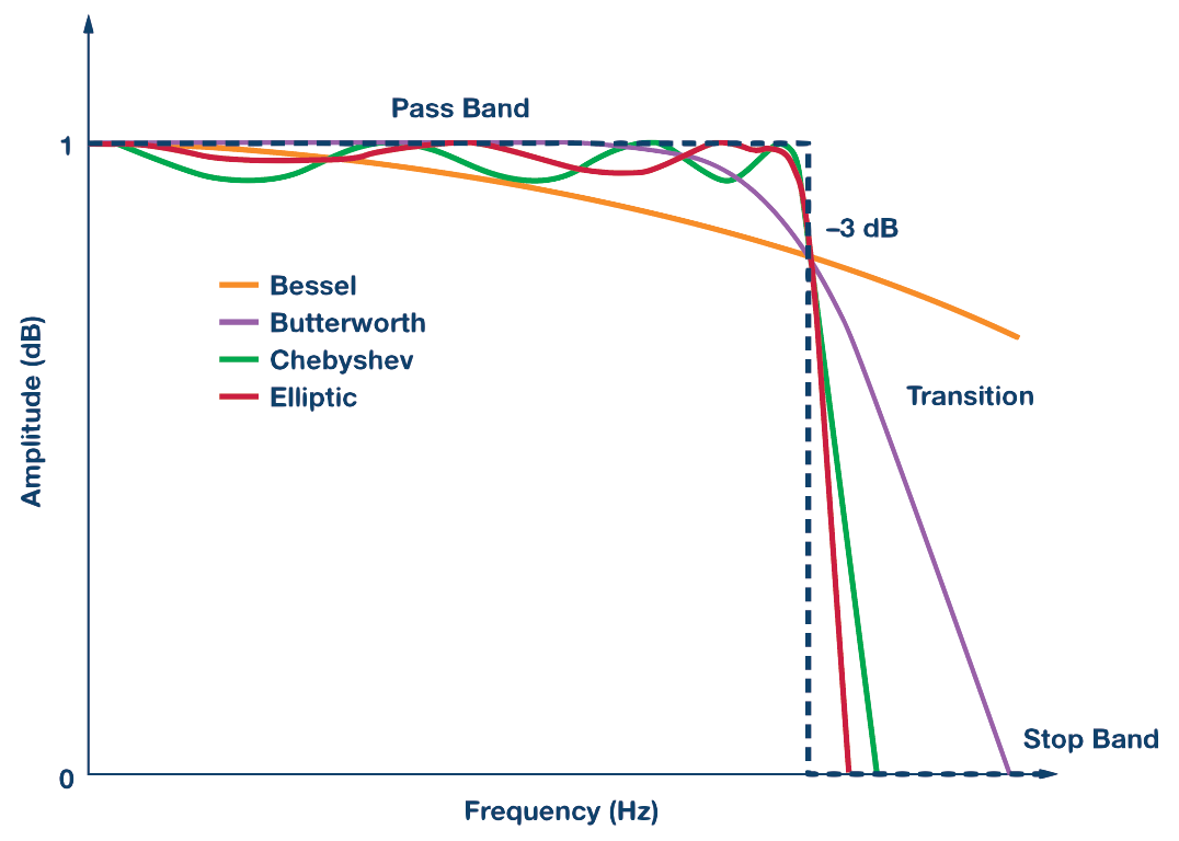
Butterworth
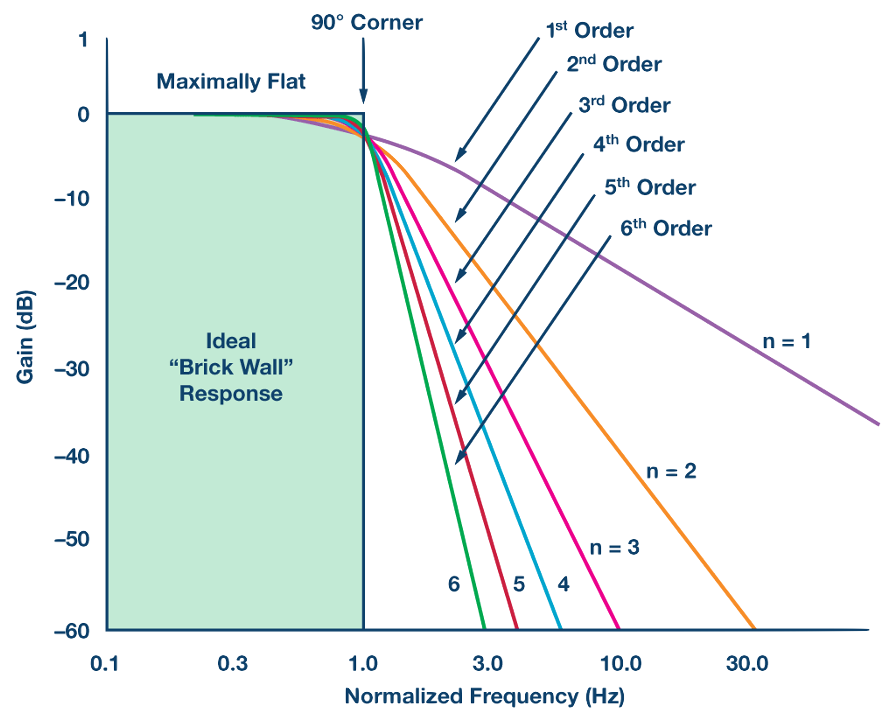
Maximally flat passband, monotonic everywhere. Gentlest roll-off, so the highest order for a given specification, and the prototype used in both examples below.
Chebyshev I
Equiripple passband, monotonic stopband. Spends the passband tolerance evenly and buys a steeper transition at lower order.
Chebyshev II
The mirror image: flat passband, equiripple stopband. Preferred when passband fidelity matters more than stopband uniformity.
Elliptic (Cauer)
Equiripple in both bands, which is the minimax solution of Lecture 7 in analog form. Lowest order of the four, worst phase behaviour.
Figure 8.1.c. The prototype families. On the left, the Butterworth magnitude of Eq. (8.2) at increasing \(N\): monotonic at every order, sharpening only as \(N\) grows. On the right, all four families at equal order, which shows where each one chooses to spend its ripple budget. Both transformations of Sections 8.2 and 8.3 are indifferent to this choice, since it is settled in the analog domain before either is applied.
8.1.3 Getting the band shape you want
Prototype tables normally use a normalized low-pass filter with unit cutoff. Standard substitutions in \(s\) convert it into a low-pass, high-pass, band-pass or band-stop response. The transformation relocates the band edges while preserving the prototype's ripple levels.
Low-pass
\(s\to\dfrac{s}{\Omega_c}\)
rescale the cutoff(8.3.a)
High-pass
\(s\to\dfrac{\Omega_c}{s}\)
invert the axis(8.3.b)
Band-pass
\(s\to\dfrac{s^2+\Omega_0^2}{Bs}\)
centre \(\Omega_0\), width \(B\)(8.3.c)
Band-stop
\(s\to\dfrac{Bs}{s^2+\Omega_0^2}\)
the band-pass, inverted(8.3.d)
Use the operations in the correct order. First form the required analog band shape using Eqs. (8.3.a)–(8.3.d), then convert the completed analog filter to digital form. For the bilinear transform, prewarp the requested digital edges before the analog band transformation.
8.2 Impulse invariance
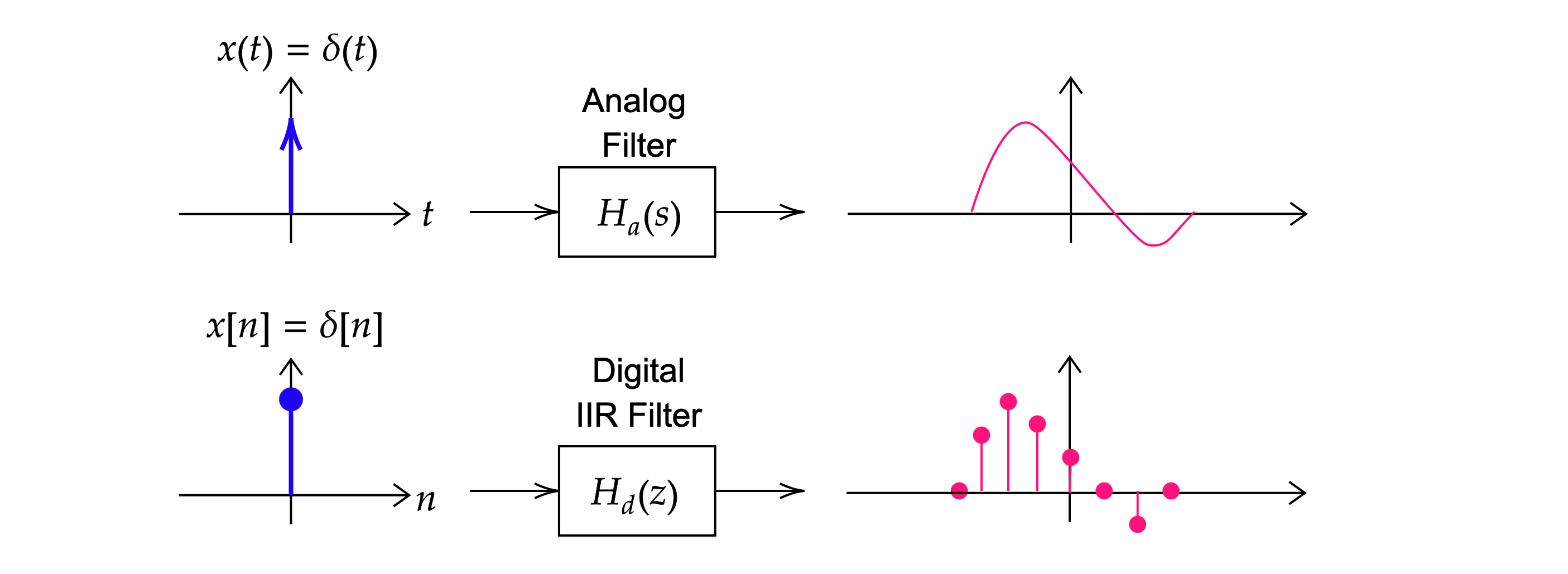
The most literal reading of "carry the analog filter into discrete time" is to keep its impulse response and simply read it at the sampling instants. That is the whole idea of impulse invariance, and everything else in this section is a consequence of it.
Figure 8.2.a. What impulse invariance asks for. The analog filter answers \(\delta(t)\) with a continuous waveform. The digital filter is required to answer \(\delta[n]\) with that same waveform, read at the sampling instants and scaled by \(T\). Note that the requirement is stated purely in the time domain; every frequency-domain consequence in this section is derived from it rather than imposed alongside it.
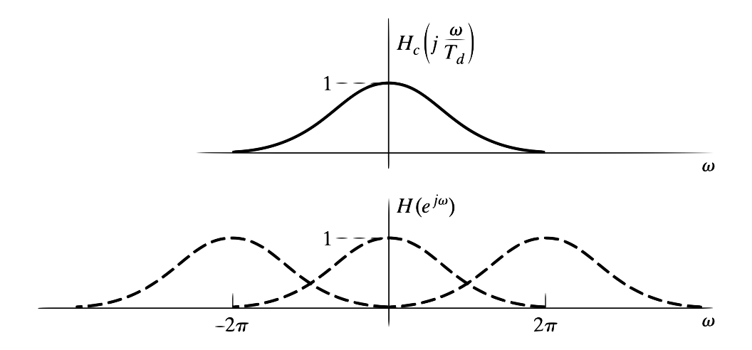
Impulse invariance samples the analog impulse response: \(h[n]=T h_a(nT)\). The interval \(T\) sets the analog-to-digital frequency scaling; in the normalized examples it is chosen conveniently. As in Lecture 3, sampling in time creates repeated spectral copies and therefore a risk of aliasing.
$$ H(e^{j\omega})=\frac{1}{T}\sum_{k=-\infty}^{\infty}H_a\!\Big(j\frac{\omega+2\pi k}{T}\Big), \qquad \omega=\Omega T \pmod{2\pi} $$
(8.5)
If the analog response were exactly zero above \(\pi/T\), the spectral copies would not overlap inside \(|\omega|\le\pi\). The digital response would then be a frequency-scaled version of the analog response:
Real analog filters are not perfectly band-limited, so neighbouring copies can overlap the baseband. The mapping remains linear, but high-frequency energy folds into lower digital frequencies. A low-pass prototype may decay enough for this error to be small. A high-pass or band-stop response retains substantial high-frequency energy, so impulse invariance is usually unsuitable.
Figure 8.2.b. The periodic sum of Eq. (8.5). The analog response at the top becomes, after sampling, the sum of shifted copies below it. Where those copies overlap they add, and the digital response departs from the analog one. This is Lecture 3's sampling aliasing seen from the filter designer's side.
To obtain a digital transfer function, first write \(H_a(s)\) in partial fractions. Each analog pole produces an exponential term in \(h_a(t)\). Sampling that exponential produces a geometric sequence with a simple \(z\)-transform:
A stable analog pole has \(\Re(s_k)<0\). Its digital image satisfies \(|z_k|=e^{\Re(s_k)T}<1\), so it lies inside the unit circle. Impulse invariance therefore preserves stability.
8.2.1 Three things Eq. (8.6) does not say
The formula maps poles, not zeros. Digital zeros appear after the partial-fraction terms are recombined over a common denominator and depend on both poles and residues. Do not map analog zeros using \(z=e^{sT}\); impulse invariance is not a complete point-by-point mapping of the two planes.
Changing the normalized value of \(T\) does not remove aliasing. The digital specification is fixed in \(\omega\), so changing \(T\) rescales both the analog band edges and the sampling boundary together. To reduce fold-back, use a higher-order prototype with faster high-frequency decay or design extra stopband margin.
Other time-domain mappings are possible. Step invariance, for example, preserves samples of the analog step response. A waveform-invariance method is useful when transient properties such as rise time, overshoot or ringing matter more than an exact frequency-axis mapping.
Advantages
Preserves the impulse-response shape exactly (up to sampling); pole mapping is a one-line formula; stable analog ⇒ stable digital, always.
Disadvantages
Aliases if \(H_a\) is not sufficiently band-limited; poor for high-pass or wideband filters, whose high-frequency content folds straight back in.
EXAMPLE 8.1 · A digital Butterworth low-pass via impulse invariance
Design a digital Butterworth low-pass (\(T=1\)) meeting \(0.89125\le|H(e^{j\omega})|\le1\) for \(0\le|\omega|\le0.2\pi\), and \(|H(e^{j\omega})|\le0.17783\) for \(0.3\pi\le|\omega|\le\pi\), via impulse invariance.
Step 1 · Neglect aliasing, map frequencies. With \(T=1\), \(\omega=\Omega\); the specification becomes an analog Butterworth specification directly: \(0.89125\le|H_c(j\Omega)|\le1\) for \(\Omega\le0.2\pi\), \(|H_c(j\Omega)|\le0.17783\) for \(\Omega\ge0.3\pi\) (valid since a Butterworth low-pass decays well before Nyquist, per Section 8.2's aliasing caveat).
Step 2 · Order (Lecture 5's Butterworth design equation). Solving \(1+(0.2\pi/\Omega_c)^{2N}=(1/0.89125)^2\) and \(1+(0.3\pi/\Omega_c)^{2N}=(1/0.17783)^2\) simultaneously gives \(N=5.886,\ \Omega_c=0.7047\); rounding up, \(\boxed{N=6,\ \Omega_c=0.7032}\). The passband specification is now met exactly and the stopband is exceeded.
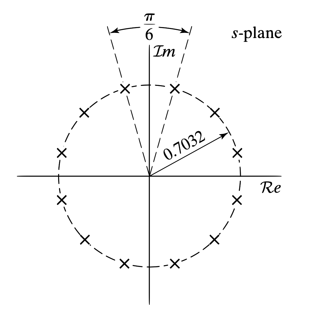
Step 3 · Analog poles. The 6 poles of \(H_c(s)H_c(-s)=1/\big(1+(s/j\Omega_c)^{12}\big)\) sit uniformly on a circle of radius \(0.7032\) in the left half-plane (Lecture 5's Butterworth pole pattern): \(-0.182\pm j0.679\), \(-0.497\pm j0.497\), \(-0.679\pm j0.182\), giving
Step 4 · Apply Eq. (8.6). Partial-fraction \(H_c(s)\), map each pole \(s_k\to z_k=e^{s_k}\) (\(T=1\)), and combine the conjugate pairs back into real second-order sections:
Figure 8.2.c. Example 8.1, Step 3. The twelve roots of \(1+(s/j\Omega_c)^{12}\) lie on a circle of radius \(\Omega_c=0.7032\), spaced by \(\pi/6\); \(H_c(s)\) claims the six in the left half-plane, and impulse invariance carries each one to \(z_k=e^{s_kT}\) inside the unit circle by Eq. (8.6).
MATLAB corner for Example 8.1
This script designs Example 8.1's \(N=6\) analog Butterworth prototype, applies impulse invariance via impinvar(), and checks the resulting digital filter against the discrete-time specification.
Goal: confirm the impulse-invariance design meets the passband/stopband targets, and show its (nonlinear, but nearly constant in-band) group delay.
impulse_invariance_demo.m
MATLAB
%% impulse_invariance_demo.m - Example 8.1's N=6 Butterworth (Eq. 8.6)
Ap = 20*log10(1/0.89125); As = 20*log10(1/0.17783);
subplot(1,3,3); grpdelay(numD, denD, 1024); title('group delay (nonlinear near transition)');
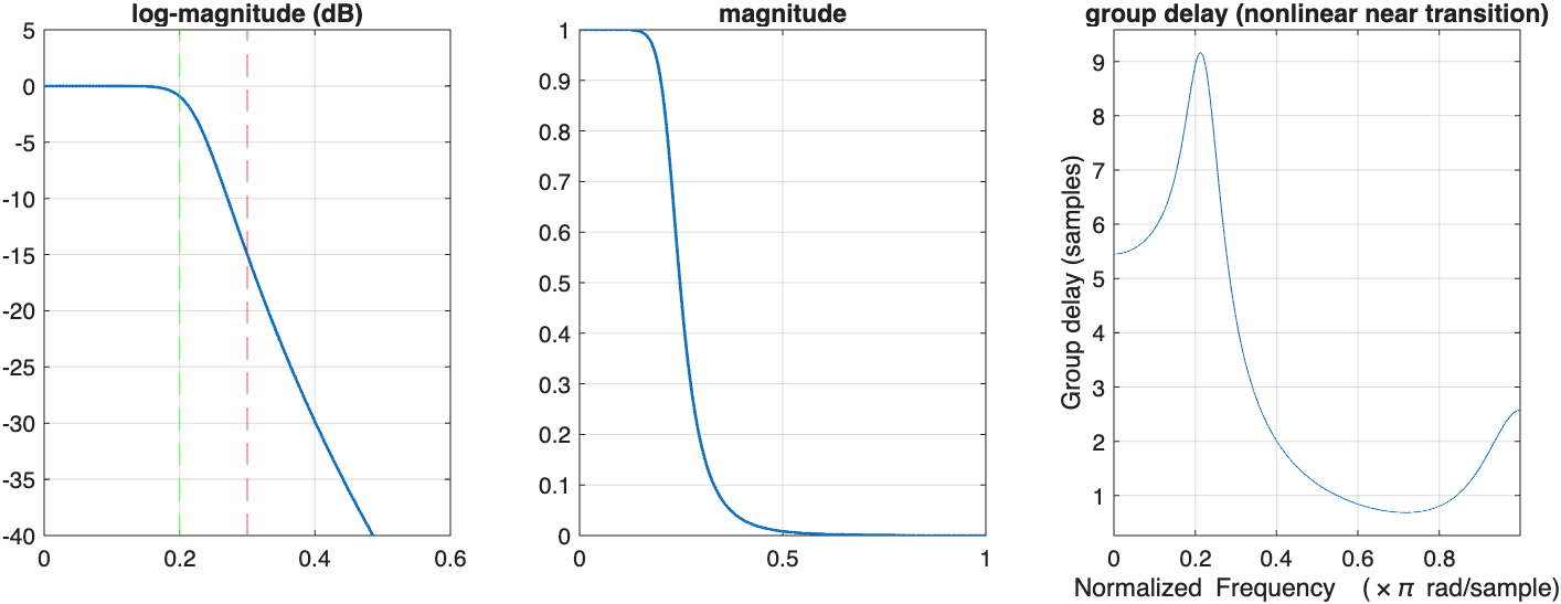
Figure 8.2.d.MATLAB verification of Example 8.1. In the left panel, the response remains within the passband limit up to \(0.2\pi\) and is more than 15 dB below the passband level by \(0.3\pi\), so both edge requirements are satisfied. The middle panel shows the smooth, monotonic roll-off expected from a Butterworth prototype. The right panel shows group delay. It is fairly steady at low passband frequencies but rises strongly through the transition band. This variation means the filter does not have linear phase; frequency components near the transition experience a different delay from components deep inside the passband.
8.3 The bilinear transform
The bilinear transform is an algebraic substitution rather than a sampling operation, so it does not create spectral copies. It maps each relevant point in the \(s\)-plane to one point in the \(z\)-plane:
Substitute \(s=\sigma+j\Omega\) into Eq. (8.7) and compare the magnitudes of the numerator and denominator. The sign of \(\sigma\) determines whether the image lies inside, on or outside the unit circle:
The complete left half-plane maps inside the unit circle, so every stable analog pole becomes a stable digital pole. Unlike impulse invariance, the mapping is one-to-one and does not fold multiple analog frequencies onto one digital frequency.
8.3.2 Frequency warping
The price of that one to one map is paid on the boundary between the two regions. Put \(z=e^{j\omega}\) into Eq. (8.7) and factor \(e^{-j\omega/2}\) out of the numerator and the denominator, which is the step that turns the algebra into a tangent:
Evaluating the inverse mapping on \(z=e^{j\omega}\) gives a purely imaginary value of \(s\), so the unit circle maps onto the \(j\Omega\)-axis. The resulting frequency relationship is nonlinear:
At low frequencies, \(\tan(\omega/2)\approx\omega/2\), so the mapping is nearly linear. As \(\omega\) approaches \(\pi\), the tangent tends to infinity. The entire unbounded analog frequency axis is therefore compressed into the finite digital interval, avoiding aliasing but producing frequency warping.
Figure 8.3.a. The bilinear map in three views. A point at angle \(\omega_0\) on the unit circle, on the left, corresponds to exactly one point \(\Omega_0\) on the \(j\Omega\)-axis, on the right. The curve in the middle is the correspondence itself, monotonic everywhere and asymptotic to \(\pm\pi\), so one trip round the circle accounts for the entire analog axis and none of it is left over to fold back.
8.3.3 Prewarping
Because the mapping is nonlinear, using the naive analog edges \(\Omega=\omega/T\) would place the final digital edges incorrectly. Prewarping applies the inverse mapping first, so the analog prototype is designed at frequencies that will transform to the required digital edges:
Prewarping makes each specified band edge land exactly at its target. Frequencies between the edges are still warped, but this does not violate an ordinary tolerance mask because the transition band is unconstrained.
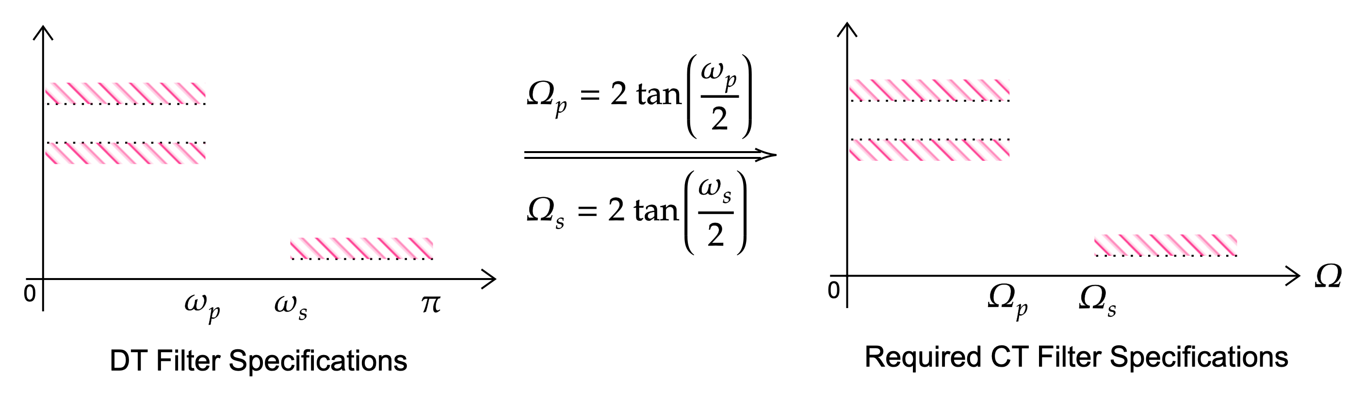
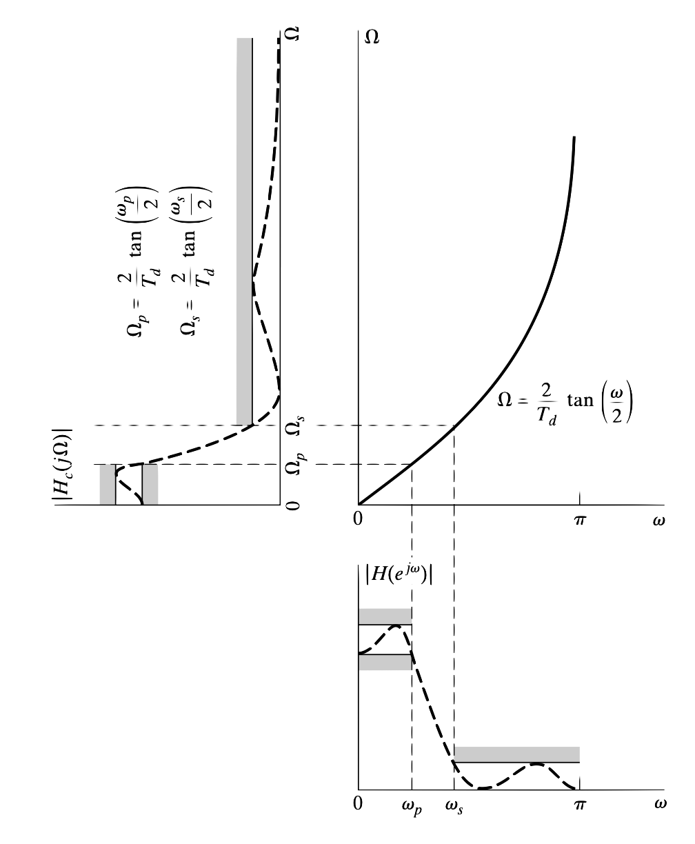
Figure 8.3.b. Prewarping viewed as a translation between specifications. The digital tolerance scheme on the left is the one that was asked for. Eq. (8.10) pushes its edges \(\omega_p,\omega_s\) outward to \(\Omega_p,\Omega_s\), and the prototype is designed against that stretched version on the right. The amplitude tolerances are carried across untouched, since only the frequency axis is distorted.Figure 8.3.c. The same operation as one picture. Start at the digital specification on the lower right, read upward through the warping curve \(\Omega=(2/T)\tan(\omega/2)\), and arrive at the analog specification on the upper left that the prototype must satisfy. Because the curve is monotonic, a tolerance band maps to a tolerance band, so a prototype meeting the upper mask is guaranteed to meet the lower one once transformed.
8.3.4 Where the poles and zeros land
The bilinear transform maps both poles and zeros. If an analog filter has fewer finite zeros than poles, its remaining zeros are regarded as lying at \(s=\infty\). These map to \(z=-1\), so a bilinear low-pass has zeros at the Nyquist frequency.
The substitution can change the overall gain, so normalize the final filter at a suitable reference frequency: DC for a low-pass, \(\omega=\pi\) for a high-pass, and the centre frequency for a band-pass.
Step-by-step BLT design procedure:
Start from a low-pass prototype \(H_{LP}(s)\) (Lecture 5).
Prewarp the digital edges to analog ones via Eq. (8.10).
Apply any needed analog frequency transformation (Lecture 5, e.g. LP→HP/BP/BS) at the prewarped edges.
Substitute the bilinear transform, Eq. (8.7).
Verify \(H(z)\) meets the original digital specification.
EXAMPLE 8.2 · A first-order Butterworth low-pass via the bilinear transform
Design a digital first-order Butterworth low-pass (\(T=2\)) with half-power frequency exactly \(\omega_c=\pi/4\), using the bilinear transform with prewarping.
Step 1 · Prewarp. Take the normalised convention \(T=2\), so the factor \(2/T=1\). Eq. (8.10) then stretches the target digital cutoff to the analog cutoff the prototype must actually have: \(\Omega_c=\tan(\omega_c/2)=\tan(\pi/8)=0.4142\ \text{rad/s}\). Designing at the naive \(\Omega_c=\omega_c=0.785\) instead would leave the digital half-power point well below \(\pi/4\).
Step 2 · Analog prototype, frequency-scaled. The first-order Butterworth prototype is \(H_{LP}(s)=1/(s+1)\), cutoff at \(\Omega=1\). Scaling it to the prewarped cutoff by the LP→LP substitution of Eq. (8.3.a), \(s\to s/\Omega_c\):
Step 3 · Substitute the bilinear transform. With \(2/T=1\), Eq. (8.7) reads \(s=(1-z^{-1})/(1+z^{-1})\). Substituting and clearing the compound fraction:
Step 4 · Read off the pole and zero. One pole at \(z=0.4142\) (inside the unit circle, as Eq. 8.8 promised for a left-half-plane analog pole) and one zero at \(z=-1\), the analog zero at \(s=\infty\) brought to Nyquist exactly as Section 8.3.4 described. The DC gain is \(2(0.2929)/(1-0.4142)=1\), so no further normalisation by Eq. (8.11) is needed here.
Step 5 · Check the specification. Evaluating at \(\omega=\pi/4\) gives \(|H(e^{j\pi/4})|=0.7071=1/\sqrt2\) to four decimals. The half-power point landed exactly on target, which is the whole return on Step 1. The same design without prewarping would have placed it at \(2\tan^{-1}(0.785)\approx0.42\pi\), missing by more than half the passband.
MATLAB corner for Example 8.2
The script designs the filter in two ways: with MATLAB's bilinear() command and by applying the prewarped substitution by hand. Comparing the two responses checks the algebra and shows why prewarping is needed to place the digital cutoff at the requested frequency.
Goal: verify \(|H(e^{j\pi/4})|=1/\sqrt2\) exactly, and show the full magnitude/phase response of the resulting one-pole digital filter.
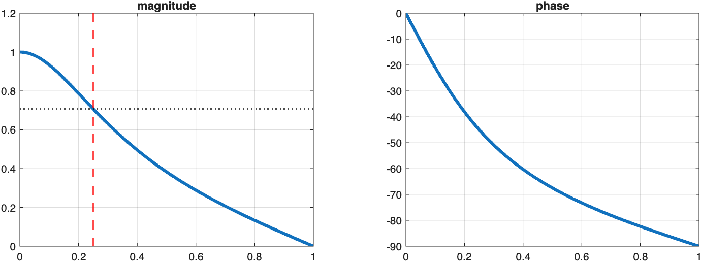
Figure 8.3.d.Checking the bilinear-transform result. In the magnitude plot, the response crosses the half-power level \(1/\sqrt{2}\), or \(-3\,\text{dB}\), at the requested digital cutoff \(\omega_c=\pi/4\). The hand calculation and MATLAB curve overlap, so both implementations give the same filter. This exact cutoff placement is the purpose of the prewarping step in Eq. (8.10); without it, frequency warping would move the crossing point. The phase changes smoothly from \(0^\circ\) towards \(-90^\circ\), as expected for a first-order low-pass IIR filter.
8.3.5 What warping does to phase
Prewarping corrects selected band edges, not the complete frequency-axis shape. In particular, an analog linear-phase response does not remain linear after the nonlinear mapping. Applying the transform to an ideal delay shows this directly:
Figure 8.3.e. Linear phase does not survive the bilinear transform. The dashed line is the phase the analog delay had, \(-\alpha\omega/T\), and the solid curve is what Eq. (8.12) returns. The two agree while \(\tan(\omega/2)\approx\omega/2\) holds, roughly over the lower third of the band, then separate without bound as \(\omega\) approaches \(\pi\). The same argument rules out a bilinear differentiator, whose defining property is a response that is linear in \(\omega\).
The bilinear transform is well suited to standard magnitude specifications because prewarping can place their important edges exactly. Impulse invariance is useful when preserving sampled time-domain behaviour or a linear frequency mapping is more important, provided the analog response decays enough to keep aliasing small. For high-pass and band-stop analog prototypes, the bilinear transform is normally required.
8.4 Changing the band shape in the \(z\)-domain
Band transformation can also be performed after a digital low-pass filter has been created. This is especially useful with impulse invariance: first transform a decaying analog low-pass prototype, then use a digital substitution to obtain the required high-pass or band-stop response.
Write \(H_{lp}(Z)\) for the digital low-pass filter already in hand and \(H(z)\) for the filter wanted. Both are rational in the inverse variable, so it is convenient to state the substitution that way as well:
The substitution \(G(z^{-1})\) must remain rational, map the unit circle onto itself, and map the inside of the unit circle into itself. These conditions preserve implementability, frequency-response meaning and stability. They lead to an all-pass substitution built from first-order factors:
The condition \(|\alpha_k|<1\) preserves stability. A single real factor maps one digital low-pass filter into another low-pass filter with a different cutoff. Let \(Z=e^{j\theta}\) denote the prototype frequency and \(z=e^{j\omega}\) the transformed frequency:
Figure 8.4.a. The frequency scale under the low-pass to low-pass substitution of Eq. (8.15). At \(\alpha=0\) the substitution is the identity and the map is the diagonal. Positive \(\alpha\) pulls the curve below the diagonal, moving the cutoff down; negative \(\alpha\) lifts it, moving the cutoff up. Every curve fixes \(\theta=0\) and \(\theta=\pi\) and stays monotonic in between, which is why a piecewise-constant response survives with its ripple heights intact and only its edges relocated.
The all-pass substitution rearranges the frequency axis without changing the prototype's magnitude values. An equiripple prototype therefore keeps the same ripple heights while its band edges move. Solving Eq. (8.15) at the desired edge determines \(\alpha\); related substitutions produce high-pass, band-pass and band-stop filters.
\(\alpha\) as above, \(k=\tan\dfrac{\omega_{p2}-\omega_{p1}}{2}\tan\dfrac{\theta_p}{2}\)
Here \(\theta_p\) is the prototype passband edge and the \(\omega\) values are the required output edges. Band-pass and band-stop mappings use two all-pass factors, so an order-\(N\) prototype becomes an order-\(2N\) filter and can shape two transitions.
EXAMPLE 8.3 · Turning a digital low-pass into a high-pass
A fourth-order Type I Chebyshev low-pass filter meets \(0.89125\le|H_{lp}(e^{j\theta})|\le1\) on \(0\le\theta\le0.2\pi\) and \(|H_{lp}(e^{j\theta})|\le0.17783\) on \(0.3\pi\le\theta\le\pi\):
Step 3 · Read what moved. The order is unchanged, since one allpass factor was used. The fourth-order zero sat at \(Z=-1\), the point that maps to \(z=+1\), so the high-pass filter has its fourth-order zero at DC, exactly where a high-pass filter needs one. The poles have moved but stayed inside the unit circle, as Eq. (8.14) guarantees for \(|\alpha|<1\).
Step 4 · Check the edge. Evaluating gives \(|H(e^{j0.6\pi})|=0.892\), which is the prototype’s passband tolerance \(0.89125\) reproduced at the new edge, and the passband ripple above \(0.6\pi\) oscillates between the same two levels as before. Only the frequency axis was rearranged; the tolerance scheme travelled with it intact.
There are two practical routes. We can change the band shape in the analog domain before converting the prototype, which is convenient when using analog design tables. Alternatively, we can convert a digital low-pass filter first and then apply a substitution in the \(z\)-domain. The second route reuses an existing digital design and is useful for high-pass or band-stop filters based on impulse invariance. In the low-pass-to-low-pass substitution, the parameter \(\alpha\) also provides a convenient way to tune the cutoff without redesigning the whole structure.
8.5 Choosing between the two methods
Both are stability-preserving, linear-algebra-simple transforms of the same analog prototype, but they disagree everywhere else:
Band-limited systems where time-domain shape matters
For most standard frequency-selective filters, the bilinear transform is preferred because it avoids aliasing and places prewarped edges exactly. Impulse invariance remains useful when preserving samples of an analog system's impulse response or transient behaviour is the main objective.
?Problems with solutions
Work each one before reading the solution.
PROBLEM 8.1
An analog pole sits at \(s_k=-2+j5\), with \(T=0.5\). Find its image \(z_k\) under impulse invariance (Eq. 8.6), and confirm it lies inside the unit circle.
\(|z_k|=e^{\Re(s_k)T}=e^{-2(0.5)}=e^{-1}\approx0.368<1\ \checkmark\), confirming Eq. (8.6)'s guarantee: \(\Re(s_k)=-2<0\) maps to a pole strictly inside the unit circle, regardless of the imaginary part.
PROBLEM 8.2
A digital specification needs edges at \(\omega_p=0.3\pi\) and \(\omega_s=0.5\pi\) with \(T=1\). A student designs the analog prototype directly at \(\Omega_p=0.3\pi\), \(\Omega_s=0.5\pi\) (no prewarping) and applies the BLT. Will the digital edges land where intended? Explain, and give the correct prewarped values.
Solution. No. Skipping prewarping means the analog edges are the unwarped values, but the BLT's own frequency relation (Eq. 8.9) will still nonlinearly compress them when mapped to \(\omega\), so the digital edges end up at \(\omega=2\tan^{-1}(\Omega/2)\), which for \(\Omega=0.3\pi\) and \(0.5\pi\) is noticeably less than \(0.3\pi\) and \(0.5\pi\) themselves (tangent-domain compression, Section 8.3.2).
Correct procedure: prewarp first, by Eq. (8.10) with \(T=1\): \(\Omega_p=2\tan(0.3\pi/2)\approx2\tan(0.4712)\approx1.019\), \(\Omega_s=2\tan(0.5\pi/2)=2\tan(\pi/4)=2\). Designing the analog prototype at these edges, then applying the BLT, lands the digital edges exactly at \(0.3\pi\) and \(0.5\pi\) as intended.
PROBLEM 8.3
A design team must convert an analog Butterworth high-pass prototype to digital. Recommend impulse invariance or the bilinear transform, and justify using Section 8.2's disadvantages list.
Solution. The bilinear transform. A high-pass prototype's magnitude does not decay at high \(\Omega\), since it stays near unity all the way to \(\Omega\to\infty\), which is precisely the case Section 8.2's disadvantages box flags as poor for impulse invariance: with substantial energy above \(\Omega=\pi/T\) and no decay to make Eq. (8.5)'s tail negligible, aliasing would be severe.
The BLT has no such exposure: its frequency mapping (Eq. 8.9) compresses the entire unbounded analog axis into \(0\le\omega\le\pi\) with no folding, so a high-pass prototype's response near \(\Omega=\infty\) simply lands, compressed but undistorted by aliasing, near \(\omega=\pi\). Prewarping (Eq. 8.10) then places the cutoff exactly where specified.
Summary and key formulas
The reference sheet: the two transforms' key equations, and the property-by-property comparison.
Impulse invariance · Eq. (8.4)
$$h_d[n]=Th_a(nT)$$
Pole mapping · Eq. (8.6)
$$z_k=e^{s_kT}$$
Aliasing relation · Eq. (8.5)
$$\omega=\Omega T\pmod{2\pi}$$
Bilinear transform · Eq. (8.7)
$$s=\dfrac{2}{T}\dfrac{1-z^{-1}}{1+z^{-1}}$$
Frequency warping · Eq. (8.9)
$$\Omega=\dfrac{2}{T}\tan(\omega/2)$$
Prewarping · Eq. (8.10)
$$\Omega_p=\dfrac{2}{T}\tan(\omega_p/2)$$
Both methods start from a Lecture 5 analog prototype and transform it, because IIR filters are essentially never optimized directly (Lecture 6, Section 6.2).
Impulse invariance samples the analog impulse response; the pole rule \(z_k=e^{s_kT}\) guarantees stability but the method can alias if the prototype is not sufficiently band-limited.
The bilinear transform is a one-to-one algebraic map: no aliasing, exact stability preservation, but a nonlinear frequency-warping relation that must be compensated by prewarping the design edges.
In practice, the BLT is the default for standard frequency-selective filters; impulse invariance is reserved for cases where the time-domain impulse-response shape itself must be preserved.
Both examples in this lecture transform a Lecture 5 Butterworth prototype, and the same recipe applies unchanged to Chebyshev or elliptic prototypes.
 MATLAB corner for Example 8.1